


Ga 100 2025 nvidia
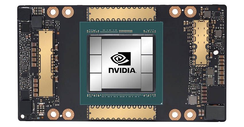
Ga 100 2025 nvidia, NVIDIA GA100 GPU VideoCardz 2025
$0 today, followed by 3 monthly payments of $11.67, interest free. Read More
Ga 100 2025 nvidia
NVIDIA GA100 GPU VideoCardz
News Corner Nvidia Ampere GA100 Brings 50 More CUDA Cores Ryzen 4000 APUs Unreal Engine 5
A100 PCIe isn t recognized by BIOS DGX User Forum NVIDIA
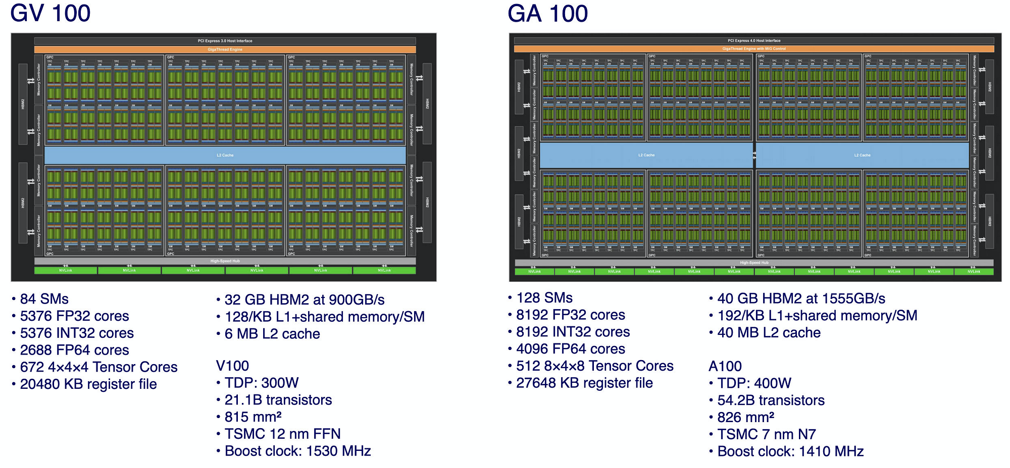
Nvidia reveals more details about the GA100 featuring 8192 Cuda
Dell NVIDIA A100 Tensor Core 40GB 400W SXM4 GPU N14YF
AI Chips Technology Trends Landscape GPU TPU FPGA
californiaworkplace.com
Product Name: Ga 100 2025 nvidiaNVIDIA Ampere GA100 Unveiled Worlds Biggest 7nm GPU Ever Built 2025, NVIDIA Ampere GA100 Unveiled Worlds Biggest 7nm GPU Ever Built 2025, NVIDIA GA100 GPU Specs TechPowerUp GPU Database 2025, NVIDIA Ampere GA100 Unveiled Worlds Biggest 7nm GPU Ever Built 2025, NVIDIA GA100 GPU Specs TechPowerUp GPU Database 2025, Nvidia Ampere GA100 GPU would get 8192 cores and boost speed up to 2025, NVIDIA Tesla A100 with GA100 Ampere GPU based on 7nm 54b 2025, NVIDIA Ampere GA100 Unveiled Worlds Biggest 7nm GPU Ever Built 2025, NVIDIA CMP 170HX mining card with GA100 GPU has a massive 2025, NVIDIA A100 Tensor Core GPU Architecture 2025, NVIDIA tipped to use its GA100 Ampere GPU in a flagship crypto 2025, Diving Deep Into The Nvidia Ampere GPU Architecture 2025, NVIDIA Ampere Architecture In Depth NVIDIA Technical Blog 2025, NVIDIA Ampere GA100 Unveiled Worlds Biggest 7nm GPU Ever Built 2025, NVIDIA GA100 GPU Specs TechPowerUp GPU Database 2025, NVIDIA Ampere GA100 Unveiled Worlds Biggest 7nm GPU Ever Built 2025, NVIDIA announces Ampere GA100 GPU VideoCardz 2025, NVIDIA Ampere GA100 GPU Unveiled Worlds Largest 7nm GPU With 54 2025, NVIDIA CMP 170HX Mining Card With GA100 GPU Comes With A Massive 2025, NVIDIA Tesla A100 with GA100 Ampere GPU based on 7nm 54b 2025, NVIDIA A100 SXM4 TENSOR CORE GPU ACCELERATOR 80GB HBM2 MEMORY BANDWIDTH 2039GB S PCI E 4.0 X16 GENERAL PURPOSE GRAPHICS PROCESSING UNIT GPGPU 2025, NVIDIA Ampere Architecture In Depth NVIDIA Technical Blog 2025, Nvidia Ampere Architecture Deep Dive Everything We Know Tom s 2025, Diving Deep Into The Nvidia Ampere GPU Architecture 2025, NVIDIA GA100 Scalar Processor Specs Sheet Released TechPowerUp 2025, NVIDIA CMP 170HX mining card with GA100 GPU has a massive 2025, NVIDIA GeForce RTX 3080 Ti GA103 Mobile GPU Flaunts Massive Die In 2025, NVIDIA DGX 100 System Featuring Eight 7nm Ampere Tesla GA 100 GPUs 2025, NVIDIA Hopper GPU Architecture and H100 Accelerator Announced 2025, Dell NVIDIA A100 Tensor Core 80GB 500W SXM4 GPU V40HX OSTK 2025, NVIDIA A100 NVIDIA 2025, NVIDIA GA100 GPU VideoCardz 2025, News Corner Nvidia Ampere GA100 Brings 50 More CUDA Cores Ryzen 4000 APUs Unreal Engine 5 2025, A100 PCIe isn t recognized by BIOS DGX User Forum NVIDIA 2025, Nvidia reveals more details about the GA100 featuring 8192 Cuda 2025, Dell NVIDIA A100 Tensor Core 40GB 400W SXM4 GPU N14YF 2025, AI Chips Technology Trends Landscape GPU TPU FPGA 2025, NVIDIA could reintroduce its Ampere GA100 GPU under CMP HX mining 2025, Gigabyte GA M61PME S2 motherboard Socket AM2 NVIDIA 6100 DDR2 100 working 2025, NVIDIA GA 100 Scalar processor specs AMD flexes next gen APU s and some more free EPIC games 2025, A2 VMs with NVIDIA A100 GPUs are GA Google Cloud Blog 2025, A2 VMs with NVIDIA A100 GPUs are GA Google Cloud Blog 2025, Nvidia Unifies AI Compute With Ampere GPU 2025, It Is What It Is Intel Is A Buy NASDAQ INTC Seeking Alpha 2025, NVIDIA Ampere Architecture In Depth NVIDIA Technical Blog 2025, Amazon Laptop Motherboard 90NR04P0 R00052 Compatible 2025, Gigabyte GA M61PME S2 motherboard Socket AM2 NVIDIA 6100 DDR2 100 2025, NVIDIA GA102 GPU Specs TechPowerUp GPU Database 2025, AI boom drove Nvidia profits up 580 last year Business 2025, A100 PCIe isn t recognized by BIOS DGX User Forum NVIDIA 2025.
-
Next Day Delivery by DPD
Find out more
Order by 9pm (excludes Public holidays)
$11.99
-
Express Delivery - 48 Hours
Find out more
Order by 9pm (excludes Public holidays)
$9.99
-
Standard Delivery $6.99 Find out more
Delivered within 3 - 7 days (excludes Public holidays).
-
Store Delivery $6.99 Find out more
Delivered to your chosen store within 3-7 days
Spend over $400 (excluding delivery charge) to get a $20 voucher to spend in-store -
International Delivery Find out more
International Delivery is available for this product. The cost and delivery time depend on the country.
You can now return your online order in a few easy steps. Select your preferred tracked returns service. We have print at home, paperless and collection options available.
You have 28 days to return your order from the date it’s delivered. Exclusions apply.
View our full Returns and Exchanges information.
Our extended Christmas returns policy runs from 28th October until 5th January 2025, all items purchased online during this time can be returned for a full refund.
Find similar items here:
Ga 100 2025 nvidia
- ga 100 nvidia
- rtx 3060 ti 12 gb
- gigabyte gtx 1660 super gaming oc driver
- gtx 780 test
- gigabyte geforce gtx 1660 super oc 6g drivers
- gigabyte geforce gtx 1660 super gaming oc 6g drivers
- nvidia 3060 12 gb
- driver gigabyte gtx 1660 super
- nvidia ampere ga 100
- 3080ti 12gb